PD Lec 29 - Cell Orientation and Flipping | Placement | VLSI | Physical Design
Lec 29-Controllers (PD,PI,PID),Control Systems || Electrical Engineering
PD Lec 55 Power Dissipation in clock tree | Clock gating | CTS | VLSI | Physical Design
PD Lec 41 - Tie Cell | tie low| tie high | VLSI | Physical Design
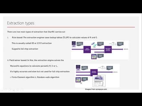
Parasitic Extraction and Back Annotation | VLSI Physical Design
PD Lec 43 - Timing Fixes in placement | Part-1 | VLSI | Physical Design
29 May 2020, VLSI Gate capacitance
PD Lec 30 - Interview Questions | VLSI | Physical Design
PD Lec 31 - Introduction to Placement | VLSI | Physical Design
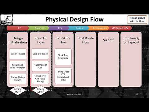
STA_L1g - Timing Check Overview in PD Flow
PD Lec 39 - CMOS Latch Up | VLSI | Physical Design
PD Lec 34 - place-opt understanding | VLSI | Physical Design
PD Lec 28 - Sanity Checks -3 | Floor-planning | VLSI | Physical Design
PD DEMO 29MAY2021
PD Lec 40 - Well Tap Cell | VLSI | Physical Design
PD Lec 32 - Placement of std cells | VLSI | Physical Design
PD Lec 24 - Power planning and power mesh creation| Floor-planning | VLSI | Physical Design
PD Lec 37 - Pin Density of std cells | VLSI | Physical Design
PD Lec 25 - Physical Only Cells | Floor-planning | VLSI | Physical Design
LEC 29 Antenna arrays I EMT I ECE EE I Crash Course I GATE 2020