LPDDR4 Design and Layout Tutorial - ADVANCED PCB Design Rules
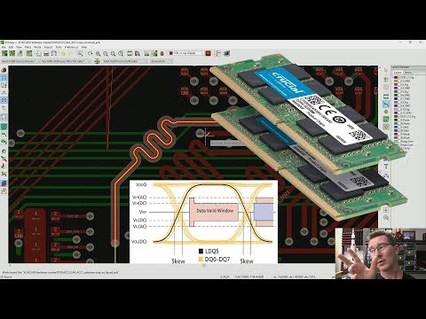
LPDDR4 PCB Design and Layout Tutorial - LPDDR4 Length Matching
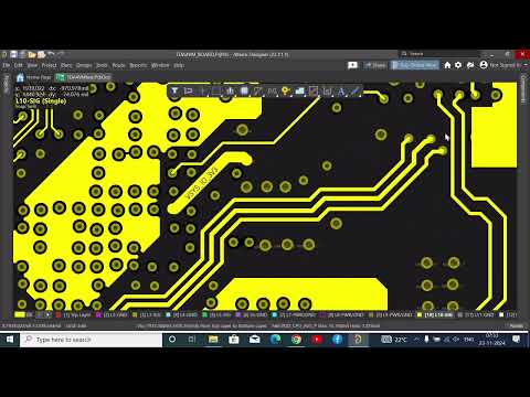
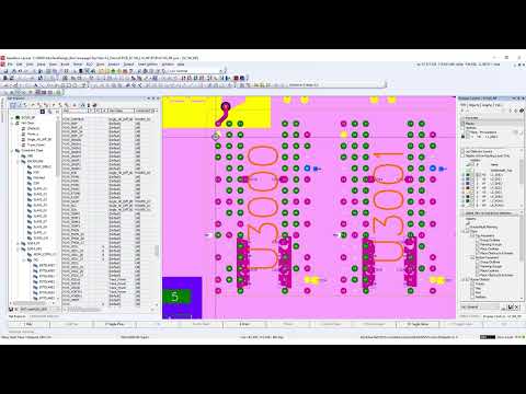
LPDDR4 Design and Layout Tutorial - How to BGA Fanout & VIAs
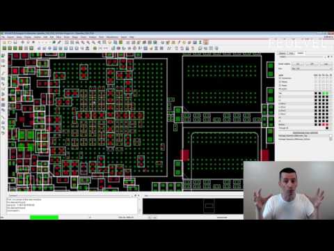
LPDDR4 PCB Design and Layout Tutorial - Power Planes Sectioning
LPDDR4 layout design
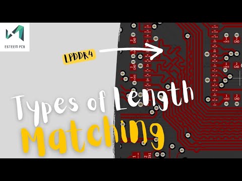
LPDDR4 Design and Layout Tutorial - Types of Length Matching
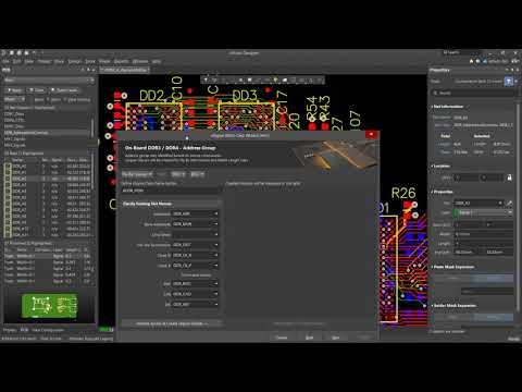
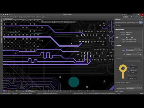
xSignals for DDR3 and DDR4 in Altium Designer | High-Speed Design
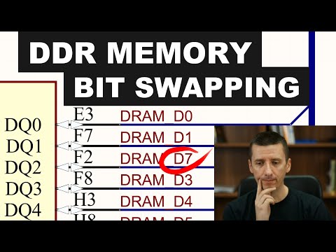
How to Do DDR Memory Bit & Byte Swapping - DDR2, DDR3, DDR4, ....
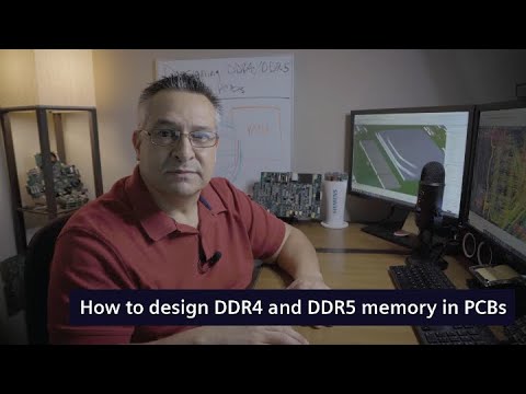
How to design DDR4 and DDR5 memory in PCBs
Setting Up DDR4 Memory Simulation | ADS | with Vandana Wylde
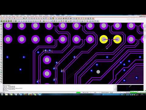
Understanding fanout and breakout on DDR4 chips | PCB design flow series: Chapter 3.2
Whiteboard Wednesdays - Understanding the In-line ECC Architecture for LPDDR4 Automotive Memories
How to Design Automatic Fanouts for BGAs in Altium Designer
EEVblog #1247 - DDR Memory PCB Propagation Delay & Layout
TIP #095: You may want to place all the components on the board before you start doing layout
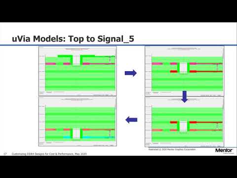
Customizing DDR4 Designs for Cost & Performance
Professional PCB Layout Design
This is why I love to design boards!
How to Route High-Speed Designs in Altium Designer
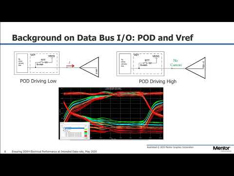
Ensuring DDR4 Electrical Performance at Intended Data-Rate