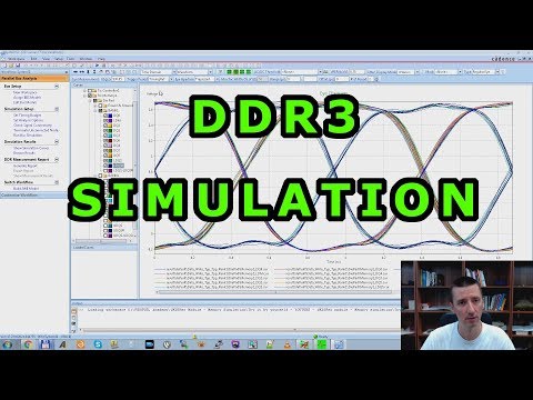
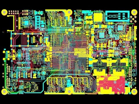
How To Do DDR3 Memory PCB Layout Simulation - Step by Step Tutorial
EEVblog #1247 - DDR Memory PCB Propagation Delay & Layout
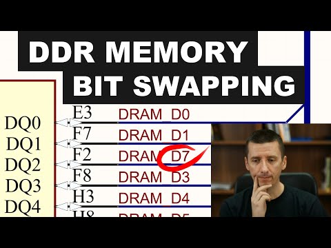
How to Do DDR Memory Bit & Byte Swapping - DDR2, DDR3, DDR4, ....
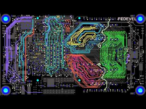
Watch routing PCB Layout with DDR3 & High Speed Interfaces
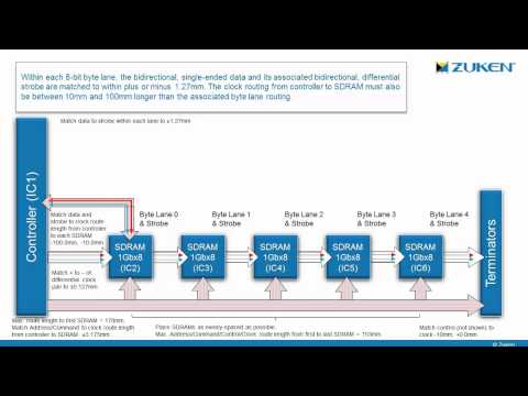
Defining and routing PCB constraints for DDR3 memory circuits - Part 1: The theory
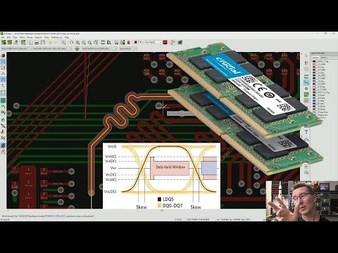
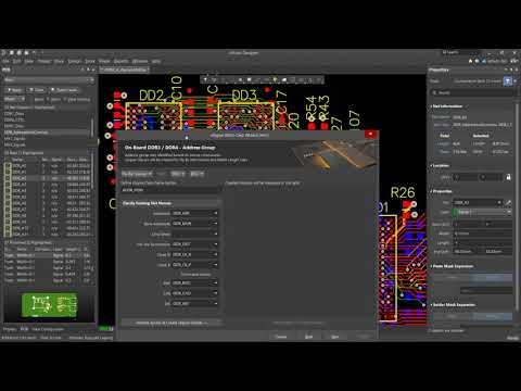
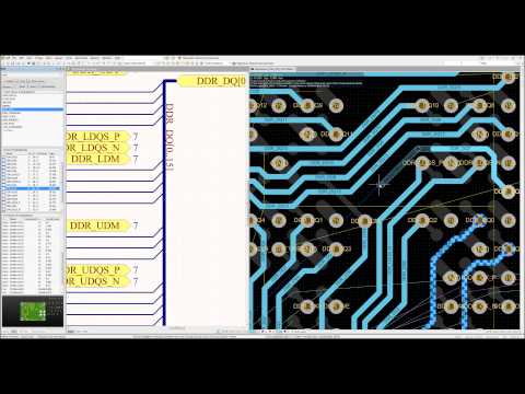
xSignals for DDR3 and DDR4 in Altium Designer | High-Speed Design
Solving DDR Memory Challenges with Advanced Simulation
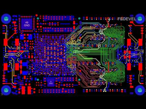
PCB Layout Fast Forward - DDR3 Memory Layout
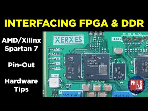
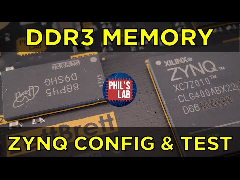
(Sponsored) Interfacing FPGAs with DDR Memory - Phil's Lab #115
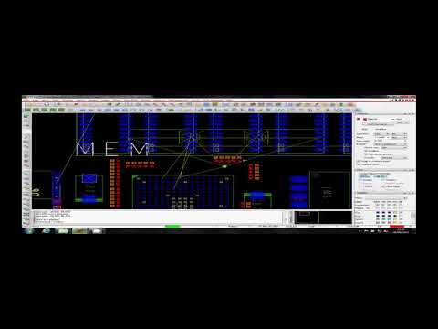
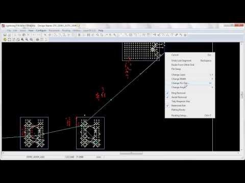
Cadence Allegro Net Scheduling DDR2, DDR3 Memory T Points Tutorial Cadence
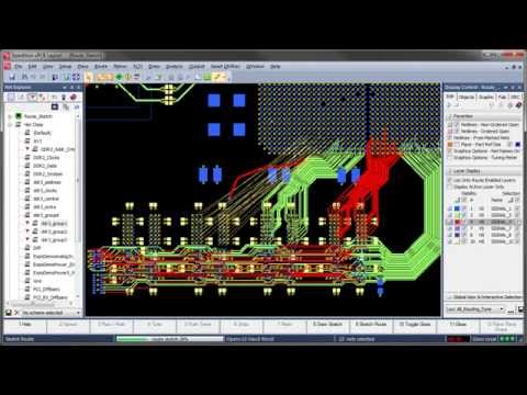
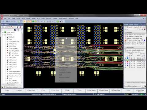
Hand Routing and Tuning DDR3 in 2 minutes 50 seconds
Routing and Tuning DDR3 in Under Three Minutes
DDR3 Memory Interface: High Performance Demo
FPGA + DDR2 layout take 1 (Failed attempt)
DDR3 Routing in Inner- versus on Outer-Layers of a PCB
(Sponsored) FPGA/SoC Board Bring-Up - DDR3 (Zynq Part 2) - Phil's Lab #97
Defining and routing PCB constraints for DDR3 memory circuits: Pt3 Routing the constraints
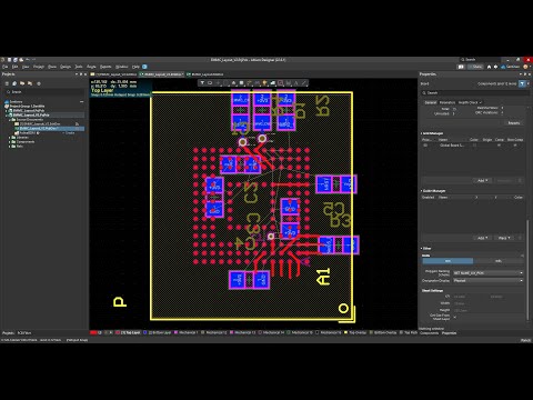
Easy BGA eMMC PCB Layout With One Simple Trick
DL Designs | High Speed DDR PCB Layout
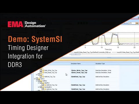
TimingDesigner Sigrity Integration for DDR3