"Effective RF And Microwave Design With KiCad" - Seth Hillbrand (KiCon 2019)
"Microwave Design with KiCad" - Darrell Harmon (KiCon 2019)
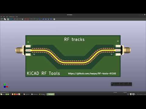
RF tools for KiCAD
Flawless PCB design: RF rules of thumb - Part 1
(1) - RF and Microwave PCB Design - Altium Academy
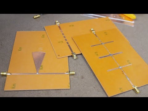
Rapid Prototyping RF Filters with Tape & QUCS
Best Practices for RF and Mixed Technology PCB Design | Sierra Circuits
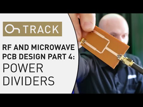
RF and Microwave PCB Design - Part 4: Power Dividers.
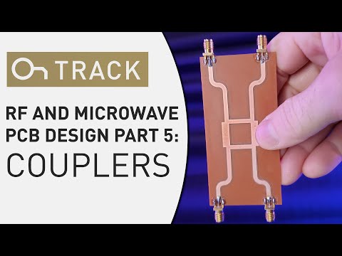
RF and Microwave PCB Design - Part 5: Couplers
KiCad Controlled Impedance Traces (e.g. 50Ω) - Phil's Lab #3
KiCad+Microstrip+OSH Park Tutorial
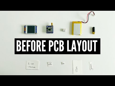
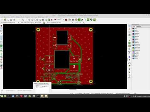
Common missing steps between the schematic and PCB layout // KiCad, PartsBox with LoRa, E-Ink, GPS
Boost Your PCB Design Productivity | 7 Best Plugins for KiCad
RF And Microwave PCB Circuit Design
KiCad v5.99: Arc/Curved Track Dragging
KiCad V6: track fillets for rounded corners
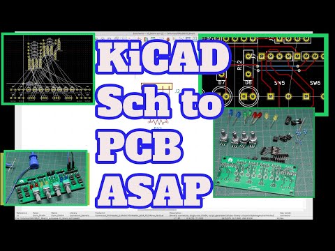
KiCAD Schematic and PCB - Quick Design Example and Build
Designing a PCB patch antenna for WiFi and Bluetooth | KiCad | Philip Salmony
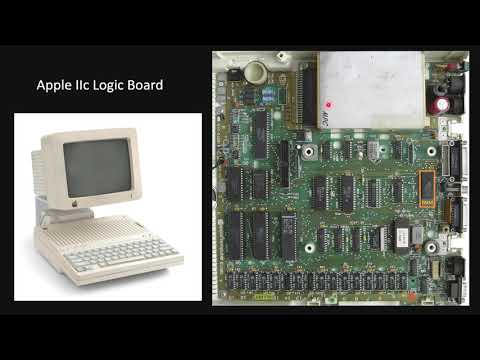
"Preserving History With KiCad" - James Lewis (KiCon 2019)
KiCad Tips zur HF Platinenkonstruktion
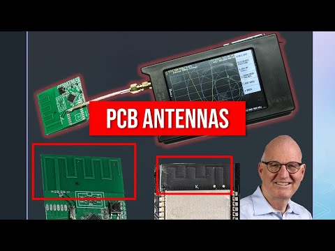
How to Design a PCB with an Antenna
Simple Universal RF Amplifier PCB Design - From Schematic to Measurements
019 Inverted-F PCB Antenna: How to tune PCB circuits using a NanoVNA
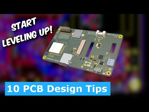
My Top 10 PCB Design Tips
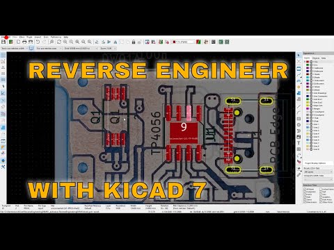
Reverse Engineer PCB With KiCAD 7 |PCB FROM PCBWAY.COM